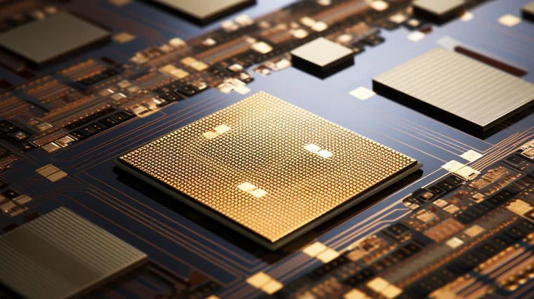
In the fast-evolving world of digital innovation, semiconductor technology is the foundation that powers everything from smartphones and supercomputers to autonomous vehicles and AI systems. Behind the scenes, a seemingly unassuming metal—titanium—plays a pivotal role in the performance, reliability, and efficiency of the semiconductors that drive our digital future.
Known for its exceptional strength, thermal stability, and corrosion resistance, titanium is far more than just a structural material. Within the semiconductor industry, titanium and its compounds are vital for advanced chip fabrication, thin-film deposition, interconnect formation, and barrier layer technologies. As the demand for faster, smaller, and more energy-efficient devices continues to rise, titanium is emerging as a critical element in the race toward next-generation electronics.
Why Titanium Is Essential to Semiconductor Manufacturing
The unique properties of titanium make it ideal for use in the highly controlled and miniaturized processes required in semiconductor fabrication. Titanium and its compounds, particularly titanium nitride (TiN) and titanium silicide (TiSi₂), are used extensively for their electrical conductivity, chemical stability, and barrier capabilities.
Core Attributes of Titanium in Semiconductors:
- Excellent adhesion to silicon substrates
- Low resistivity (for conductivity)
- High thermal stability (crucial for processing at high temperatures)
- Strong diffusion barrier properties
- Compatibility with sub-nanometer scale production
These qualities make titanium a preferred material for a variety of roles in the microchip production process.
Titanium in Thin-Film Deposition and Barrier Layers
As transistor sizes shrink to the nanometer scale, managing electrical pathways becomes increasingly complex. Titanium and its compounds help maintain signal integrity and prevent contamination between metal layers in integrated circuits.
1. Titanium as a Barrier Metal
Titanium is widely used as a barrier layer to prevent diffusion of metals (such as copper or aluminum) into silicon substrates. This is essential for preserving the performance and longevity of the chip.
- Titanium layers are deposited between silicon and metallization layers
- They act as a physical and chemical buffer, resisting high temperatures and chemical reactions
- This enhances the reliability and durability of semiconductor devices
2. Titanium Nitride (TiN) Coatings
Titanium nitride, a golden-colored ceramic material, is prized for:
- Low electrical resistivity
- High thermal and chemical stability
- Excellent conformality on complex geometries
TiN is deposited using techniques like physical vapor deposition (PVD) or atomic layer deposition (ALD) and is used as a gate electrode material, diffusion barrier, and even as a hard mask in etching processes.
Titanium Silicide (TiSi₂) in Contact Formation
In advanced microprocessors and memory devices, efficient current flow through the transistor’s contact points is critical. Titanium silicide (TiSi₂) is used to form low-resistance electrical contacts.
Why Use TiSi₂?
- It reduces the contact resistance between metal lines and silicon
- Improves switching speed of transistors
- Withstands thermal cycling during high-volume chip fabrication
This material is particularly valuable in CMOS technology, where fast switching and low power consumption are top priorities.
Advanced Lithography and Patterning Support
As semiconductor manufacturers push below 5nm technology nodes, precision patterning becomes more complex. Titanium-based materials support hard masks used during lithography and etching processes.
- TiN is commonly used in multi-patterning techniques to help define intricate circuits
- It provides etch selectivity and dimensional control, ensuring minimal distortion during production
These capabilities are crucial in maintaining yield and quality at extremely small geometries.
Titanium in High-k/Metal Gate (HKMG) Technology
With traditional silicon dioxide gate dielectrics reaching their physical limits, the semiconductor industry has adopted high-k/metal gate stacks to reduce leakage currents and power consumption.
Titanium’s Role in HKMG:
- Acts as a metal gate electrode material, often in combination with hafnium-based dielectrics
- Offers compatibility with high-k materials
- Enhances performance and scalability of advanced transistor designs
Titanium helps enable smaller, faster, and more energy-efficient transistors, making it an indispensable component in state-of-the-art chip manufacturing.
Emerging Applications of Titanium in Semiconductor R&D
As semiconductors evolve to include quantum computing, AI accelerators, and 3D-stacked architectures, titanium is playing a growing role in experimental and future-forward applications.
1. 3D Integration and Packaging
Titanium is used in through-silicon vias (TSVs) and micro-bumps to enable vertical stacking of dies. These structures require robust interconnects and thermal management, both of which benefit from titanium’s properties.
2. Flexible and Wearable Electronics
Titanium thin films are being explored for use in flexible substrates for wearable devices, medical sensors, and IoT components due to their mechanical flexibility and biocompatibility.
3. Quantum and Neuromorphic Computing
In neuromorphic and quantum chip designs, where extreme precision and material stability are vital, titanium offers promising avenues for low-resistance connections and novel logic devices.
Sustainability and Process Optimization with Titanium
Sustainability is a rising concern in semiconductor fabrication. Titanium contributes to energy-efficient production and process optimization in several ways:
- Low material consumption: Titanium is used in ultra-thin layers, minimizing resource use
- Recyclability: Titanium scrap and waste from deposition processes can be recovered and reused
- Long-lasting tooling: Titanium coatings extend the life of etching chambers and deposition tools, reducing maintenance and downtime
By supporting long-term operational efficiency, titanium helps chipmakers reduce environmental impact while maximizing output.
Challenges and Future Directions
Despite its many benefits, using titanium in semiconductors comes with challenges:
1. Deposition Complexity
Achieving uniform and ultra-thin titanium layers requires precise process control using PVD, CVD, or ALD technologies. Manufacturers are investing in automation and AI-driven process tuning to improve yields.
2. Cost and Material Availability
Titanium compounds and sputtering targets can be expensive. Ongoing R&D aims to optimize titanium use, recycle more effectively, and develop alternatives where possible—though titanium remains difficult to replace in key roles.
3. Integration with New Materials
As semiconductors adopt new materials like graphene, 2D semiconductors, and organic compounds, compatibility with titanium will need continuous innovation and adaptation.
Conclusion: Titanium—The Unsung Hero of Microchip Innovation
Though it often works behind the scenes, titanium is an essential element in building the tiny but powerful chips that fuel our digital age. From enabling low-resistance interconnects and thermal barriers, to enhancing gate stacks and supporting advanced lithography, titanium’s impact on semiconductor technology is vast and growing.
As the industry continues to scale down while pushing performance up, titanium’s role will only become more critical. In the race for smaller, faster, and more energy-efficient electronics, titanium remains one of the most reliable and innovative allies in modern semiconductor manufacturing.

Also Read :